![]()
EECS 412 Class
Handouts
![]()
Section 1.4: Amplifiers
Section 1.5: Circuit
Models for Amplifiers
Section
1.6: Frequency
Response of Amplifiers
Section
2.1: The Op-Amp Terminals
Section 2.2: The Ideal Op-Amp
The Ideal Operational
Amplifier
Section 2.3: The Inverting Configuration
Analysis of the
Inverting Amplifier
Ri and Ro
of the Inverting Amplifier
Section 2.4: Other Applications of the Inverting
Configuration
An
Application of the Inverting Integrator
Section 2.5: The
Non-Inverting Configuration
The NonInverting
Configuration
Section 2.6: Examples of Op-Amp Circuits
Example: A
Non-Inverting Network
Example: Another
Inverting Network
Superposition and
OpAmp Circuits
Differential and
Common Mode Gain
Section 2.7: Effect of Finite Open-Loop Gain and
Bandwidth on Circuit Performance
Example: The
Gain-Bandwidth Product
Section 2.8: Large-Signal Operation of Op-Amps
Section 2.9: D.C. Imperfections
Example: The Input
Offset Voltage
Reducing
the Effect of Input Bias Current
Section 4.6: Analysis of Transistor Circuits at DC
BJT Gain and the
Active Region
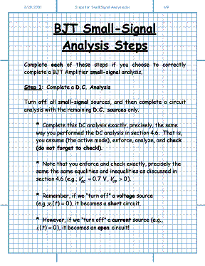
Steps for
DC Analysis of BJT Circuits
Hints for DC Analysis of BJT Circuits
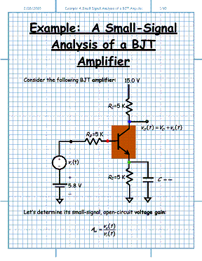
Example:
DC Analysis of a BJT Circuit
Example:
Another BJT Circuit Analysis
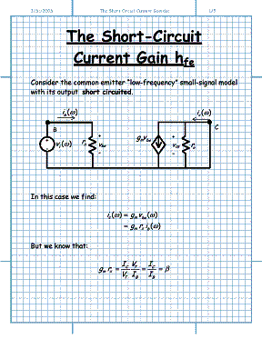
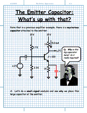
Section 4.7: The Transistor as an Amplifier

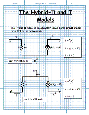
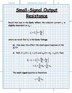
Section 4.8: Small-Signal Equivalent Circuit Models
Section 4.9: Graphical Analysis
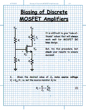
Section 4.10: Biasing the BJT for Discrete-Circuit
Design
Section 4.11: Basic Single-Stage BJT Amplifier
Configurations

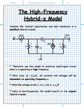
Section 4.15: Complete Static Characteristics, Internal
Capacitances, and 2nd Order Effects
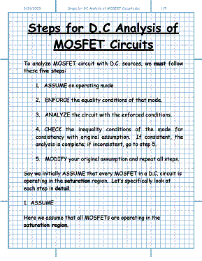
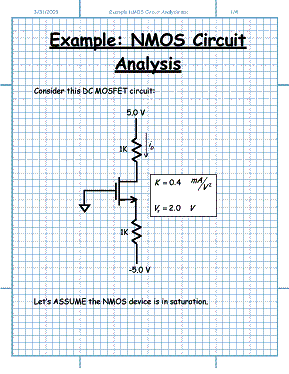
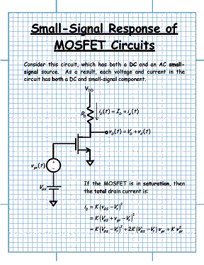
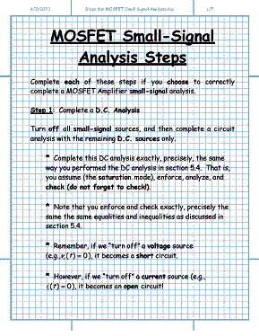
Section 5.4: MOSFET Circuits at DC
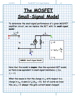
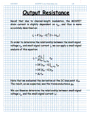
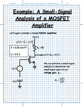
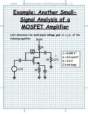
Section 5.5: The MOSFET as an Amplifier
Section 5.6: Biasing in
NMOS Amplifier Circuits
The remainder of the course handouts are
handwritten and cannot be placed on the web!