1. Set up the circuit shown below on a solderless breadboard.
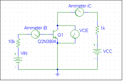
Set iB = 10 m A. Vary VCC from 0 to 10 V in 0.5 V steps. Measure the corresponding iC and VCE. (IB should remain constant).
Plot iC vs. vCE.
Repeat the above step for iB = 30 m A.
Use the graph to find b and Early voltage, VA.
Also indicate the different regions on the graph.
2. Set up the common-emitter circuit shown below.
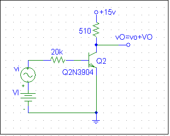
VI = 3 V, vi = 0.1 sin (2p f t), f = 1 kHz.
- Start with only the dc input. Is Q2 in active mode? Explain.
- Find the operating point of Q2 (IE, IB, IC, VE, VB, VC ). Adjust VI so that VO = 5 V. Find the operating point again. Also find the b. Is the measured b in the expected range?
- Add the ac input voltage. Measure the magnitude of the small signal voltage gain (vo/vi) and current gain (io/ii) of the circuit.
- Change VI to -3 V. What happens to VO? Explain.
- Pick one of the active-region operating points, and adjust VI and VCC to bias your circuit at this point. Then measure the magnitude of the voltage gain, current gain, input resistance, and output resistance.
- Let vi be a triangular wave with an initial amplitude of 0.2 Vp-p. While observing the output on an oscilloscope as the amplitude of vi is increased, determine the maximum value vi that results in no observable distortion. Indicate whether the distortion is caused by the saturation region or the cut-off region. To illustrate the distortion, plot vi and vo vs. time on the same graph.
[rout is obtained by applying an ac test voltage on the output, with a capacitor (100 mC) placed between vo and vtest. vi is turned off. rout = vtest / itest]
3. Set up the common-collector circuit shown below.
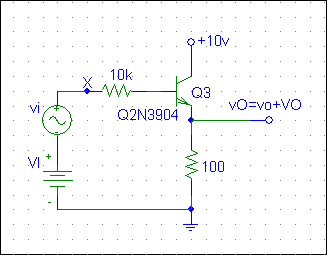
VI = 3 V, vi = 0.2 sin (2p f t), f = 1 kHz.
- Start with only the dc input voltage (i.e., vi = 0). Is Q3 in active mode? Explain.
- With VI = 3 V, and then adjust it so VO = 2 V, measure the operating point of Q3 (IE, IB, IC, VE, VB, VC ). Also find the b . Is the measured b in the expected range?
- Include the ac input voltage. Measure the ac voltage gain (vo/vi) and current gain (io/ii) of the circuit.
- Measure rin for the circuit by measuring the ac voltage and current at node X.
- Measure the output resistance looking into node vo. (Refer to 2(e)).
- Observing the output voltage on an oscilloscope as the amplitude of vi is increased from 0.2 Vp-p to 2 Vp-p. Sketch the output for both extremes of the input. What happens at the output for the 2 Vp-p amplitude sinusoidal input? Remember to keep VI at the value set in (b).